Colpitt’s Oscillator is an excellent circuit and is widely used in commercial signal generators upto 100MHz.
It consists of a single-stage inverting amplifier and an LC phase shift Network.
The two capacitors 
 and
and  provides potential divider used for providing
 . is the feedback element and which provides positive feedback required for sustained Oscillations.
The amplifier circuit is a self-Bias Circuit with 
 ,
,  and parallel combination of
 with
with 
 .
.

 is applied through a resistor
  (or) RFC choke some times. This RFC choke offers very high impedance to high frequency currents.
value has chosen in such a way that it offers high impedance. Two coupling Capacitors 
 and
and  are used to block d.c currents, that means they do not permit d.c currents into tank circuit.
These capacitors and provides a path from Collector to Base through LC Network.
when is switched on , a transient current is produced in the tank circuit an consequently damped oscillations are setup in the circuit.
The oscillatory current in the tank circuit produces a.c voltages across and . If terminal 1 is more positive w.r. to 2 , then voltages across and are opposite thus providing a phase shift of 
 between 1 and 2.
as the transistor is operating in CE mode , it provides a phase shift of .
Therefore the over all phase shift provided by the circuit results 
 which is an essential condition for developing oscillations.
If the feedback is adjusted so that the loop gain 
 then then the circuit acts as an Oscillator.
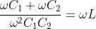
The frequency of oscillation depends on the tank circuit and is varied by gang (or) group tuning of and means 
 .
.
working:-
The capacitors and are charged by and are discharged through the coil 
 setting up of oscillations with frequency

%7D) .
.
these oscillations across are applied to the Base-Emitter junction and the amplified version of output is collected across Collector (the frequency of amplifier output is same as that of input of the amplifier) .
This amplified energy is given back to tank circuit to compensate losses.
therefore un damped oscillations results in the circuit.
Derivation for frequency of oscillations:-
chose 
 for sustained oscillations.
Analysis(Qualitative):-
if 
 ,
,  and
and  are pure reactive elements such that
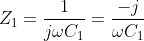 ,
, 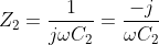 and
and 
 .
.
from the general condition for an Oscillator


+Z_%7B1%7DZ_%7B2%7D(1+h_%7Bfe%7D)+Z_%7B1%7DZ_%7B3%7D=0) .
.

+%5Cfrac%7Bj%5E%7B2%7D%7D%7B%5Comega&space;%5E%7B2%7DC_%7B1%7DC_%7B2%7D%7D(1+h_%7Bfe%7D)-%5Cfrac%7Bj%7D%7B%5Comega&space;C_%7B1%7D%7D.j%5Comega&space;L=0)
find the real and imaginary parts,

h_%7Bie%7D-%5Cfrac%7B1%7D%7B%5Comega&space;%5E%7B2%7DC_%7B1%7DC_%7B2%7D%7D(1+h_%7Bfe%7D)+%5Cfrac%7BL%7D%7BC_%7B1%7D%7D=0)
equating imaginary part to zero 
=0) , since
, since 
 .
.

 .
.
after simplification

%7D) .
.
by substituting 
 results .
substituting the value of 
 in the real part gives
 . this is the condition for sustained oscillations.
Note: There is a rating embedded within this post, please visit this post to rate it.


